Two weeks ago during their GDC Keynote Nvidia announced the first few video cards from their upcoming 4000 series of GPUs based on the Ada Lovelace architecture. They announced the RTX 4090 and two RTX 4080 cards, one with 16GB of VRAM and the other with 12GB which in addition to the memory those cards have a different base GPU as well. But today the performance embargo for the RTX 4090 is lifted so we are going to focus on that and the RTX 4090 will be available for sale tomorrow should you be interested in picking one up. Today I’m going to dive into the 4000 series of cards to tell you a little about them if you haven’t read about them yet then we will check out the RTX 4090 Founders Edition closer and then dive into testing, it’s a lot to go over so let’s dive in!
Product Name: Nvidia RTX 4090 Founders Edition
Review Sample Provided by: Nvidia
Written by: Wes Compton
Amazon Affiliate Link: HERE
What is the 4000 Series all about
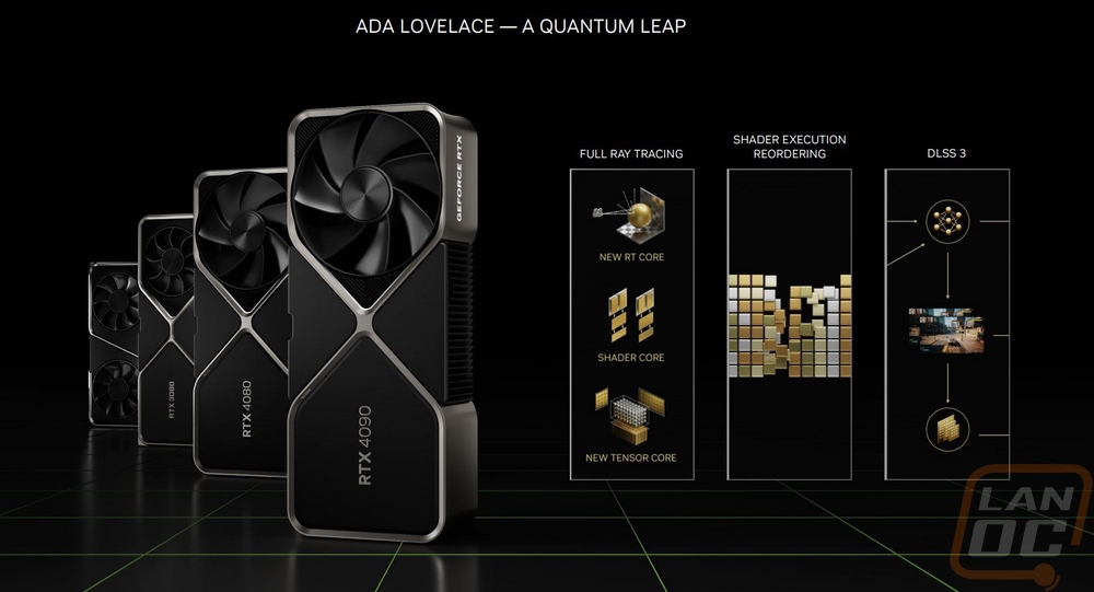
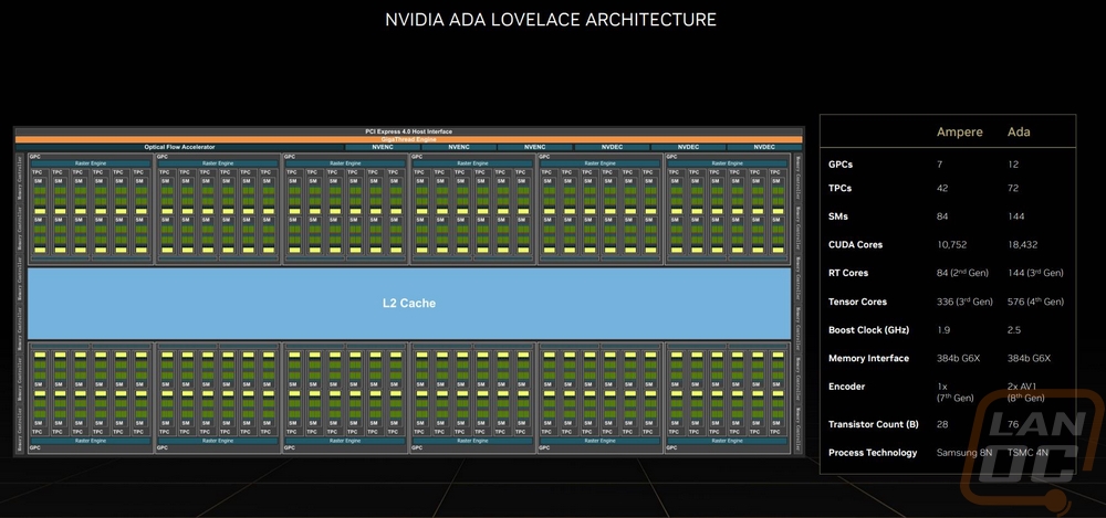
Nvidia’s 3000 Series of cards launched back in September of 2020 and with that brought their Ampere microarchitecture, the Samsung 8N manufacturing process, and a completely new card design as well. Here we are two years later but it feels like it's been four years and a lot has changed and a lot is changing with the new 4000 Series of cards. Ampere is in the mirror and the new cards are now based on the Ada Lovelace microarchitecture which is named after the English mathematician Ada Lovelace who is often regarded as the first computer programmer. The new Ada Lovelace based GPUs would also be produced by TSMC’s 4N process which is a 5 nm process and itself brings the possibility of efficiency improvements alongside the new microarchitecture. So what all has changed with Ada Lovelace?
The new microarchitecture has a new fourth-generation tensor core design and a new third-generation ray tracing core design to continue to expand on the ray tracing performance established over the previous two generations of cards and the AI processing originally introduced with Volta. The new tensor cores are capable of up to 1400 Tensor TFLOPs, four times that of the 3090 Ti which alongside the introduction of DLSS 3 are set to bring huge leaps in DLSS performance. Lovelace now has what they call Shader Execution Reordering or SER that can reschedule the workload to ensure that similar shaders are being processed together which helps a lot with processing ray tracing by allowing the multiprocessors to work more efficiently.
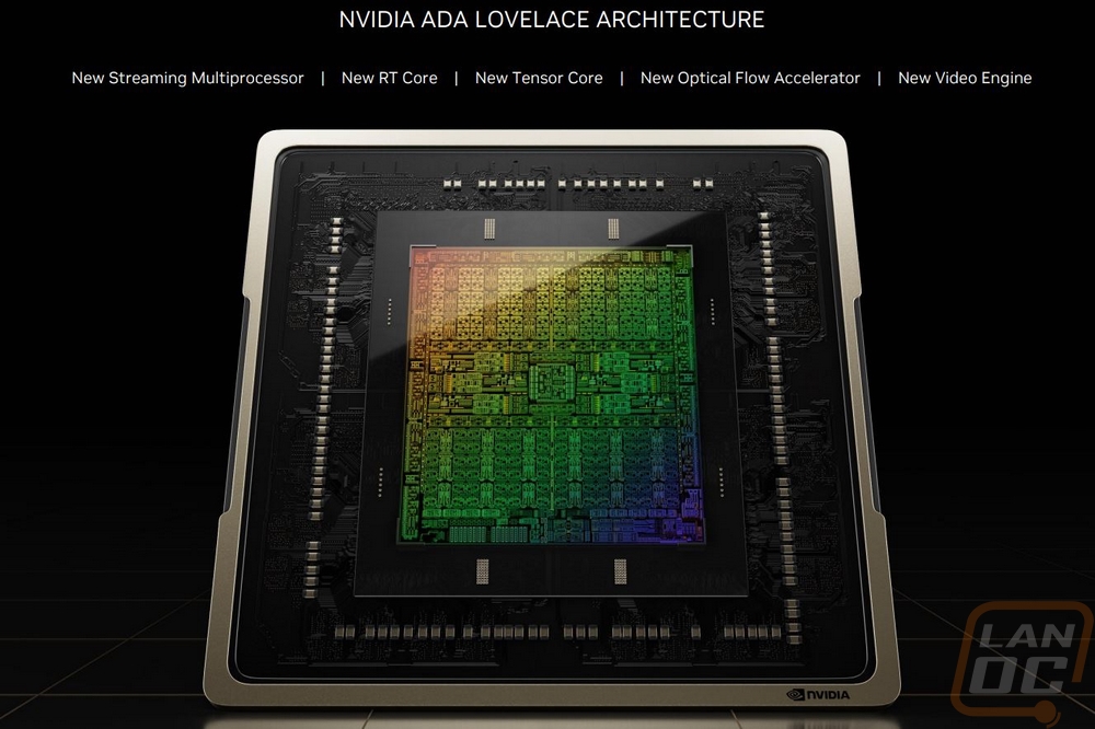
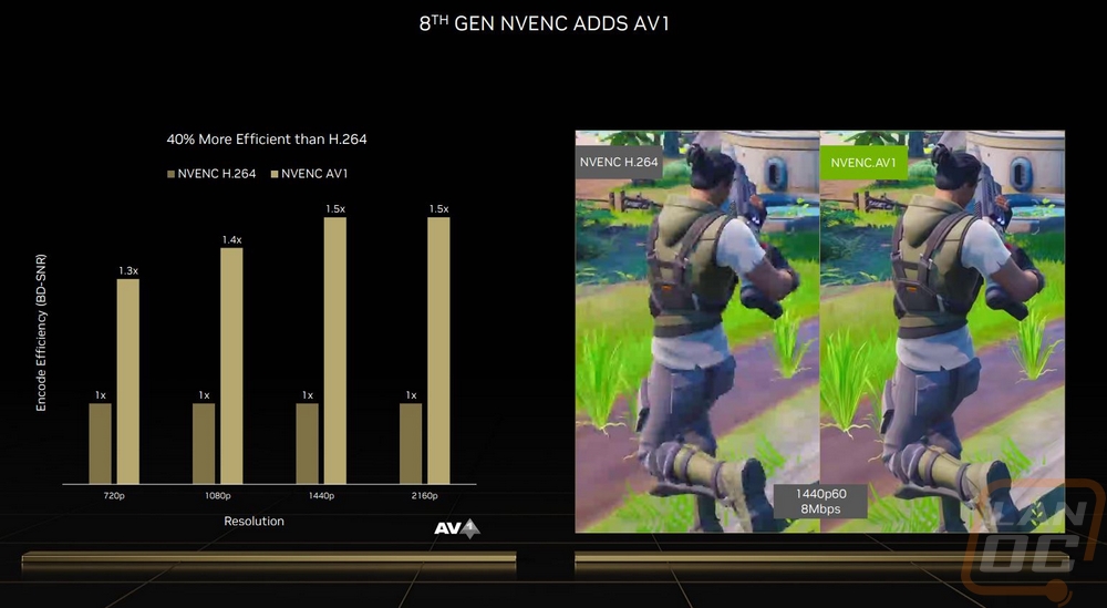
Nvidia has also doubled up on the AV1 processing which was added last generation with the new cards having two AV1 processors. This is important because AV1 which is a royalty-free video encoding format which is also 30% more efficient than H.265 meaning with it you can stream higher bitrate video with less bandwidth. AV1 is set to be added to streaming tools like OBS and Discord as well as video production tools as well and having two encoders in NVENC will be huge.
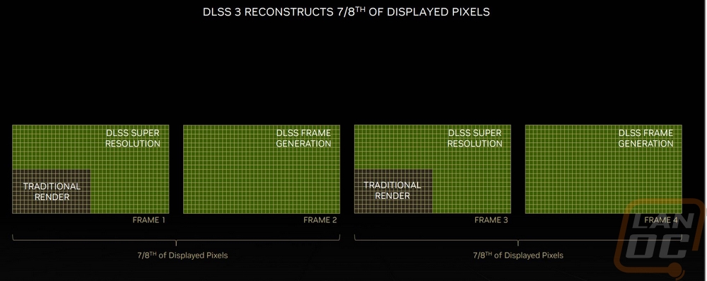
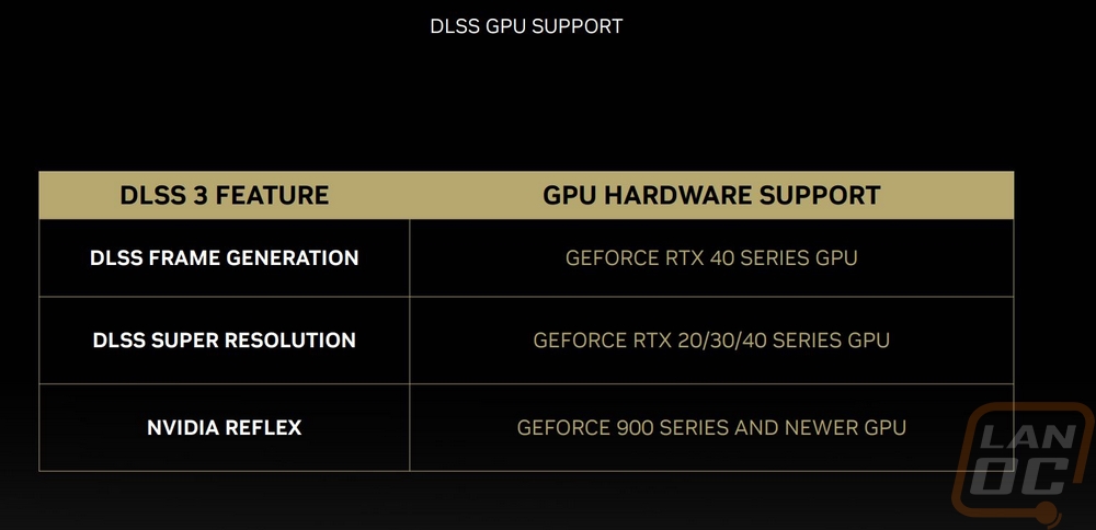
DLSS 3 in itself is a big change and sadly it is exclusive to the new 4000 series cards because it relies on Lovelace’s new Optical Flow Accelerator as well as the new much more powerful Tensor Cores. On the plus side though if you have a previous generation Nvidia card DLSS 3 is an extension of DLSS 2 so games that add DLSS 3 will also have DLSS 2. DLSS 3 combines the DLSS Super Resolution from DLSS 2 and adds in DLSS Frame Generation. So previously with DLSS Super Resolution, each frame generated would use the AI tensor cores to scale the resolution up to get the detail you want while keeping the processing time down. DLSS Frame Generation on the other hand takes every other frame and generates a complete frame. With the two combined DLSS 3 is reconstructing 7/8th of the pixels displayed. The DLSS Frame Generation has a really interesting side effect as well that DLSS Super Resolution didn’t have. When you are rendering an entire extra frame like that, it also brings performance improvements to games that are CPU limited which means that games that are CPU limited could implement DLSS 3 and see up to twice the frame rate improvement.
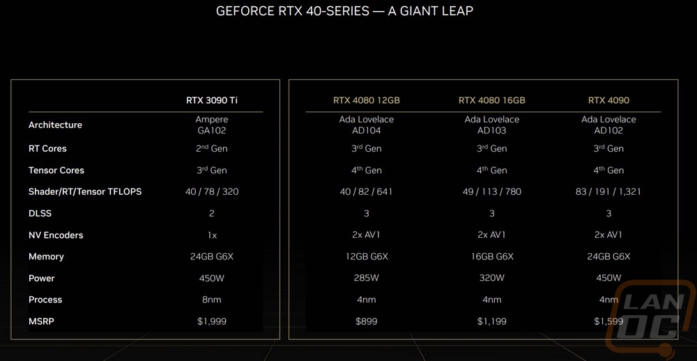
As far as 4000 Series cards, Nvidia did announce three different cards with their announcement of Ada Lovelace and the new generation of cards. The flagship of those cards is the RTX 4090 and then they have two different RTX 4080 models which have caused some confusion and uproar in the hardware community. All three are based on Ada Lovelace but they are on three different GPU variations. The RTX 4090 is on the AD102, the RTX 4080 16GB is on the AD103, and the RTX 4080 12GB is on the AD104. I will dive more into the new 4080 models as those launch later but obviously with them sharing the same name but having different memory levels has happened in the past with Nvidia cards but never before have those different memory capacities had a completely different GPU or memory controller which they have done here. The “104” designation on the GPU is normally seen on the xx70 cards which have had some people accusing Nvidia of rebranding their xx70 up to an xx80 so they could raise pricing but on the previous calls with Nvidia, they have responded that they felt that the cards performance was that of an xx80 card and that it should get the naming. I agree that the naming is going to be confusing, I don’t think we will know on the rest until the 4080s are tested and more importantly until we see the xx70 card from the 4000 series which may be a while.
With our focus on the new RTX 4090 today I put together a table to compare its specs alongside the RTX 3090 Ti which was the former flagship, the RTX 3090, and the RTX 3080 Ti which are all Ampere-based cards at the top of Nvidia’s lineup over the last few years. It is interesting right in the top few specifications to see that the RTX 4090 has 11 graphics processing clusters whereas all three of the other cards had 7. This means the RTX 4090 is using 11 out of the 12 GPCs that Ada Lovelace has on its full size. TPCs or texture processing clusters and SMs (streaming multiprocessors) also scaled up which the TPC consists of SMs inside so that isn’t a surprise. This leads us to the big number though, all together the RTX 4090 has 16384 CUDA cores which is 52% more than the RTX 3090 Ti, which is on top of the architectural improvements as well. So with these numbers in mind, we know that each SM has a total of 128 CUDA cores. The 512 new 4th generation Tensor cores tell us each SM has 4 total and then the 128 total RT or ray tracing cores tells us each SM also has one ray tracing core as well.
On top of the brute force rise in processing power with more CUDA, Tensor, and RT cores as well as architectural improvements with the new tensor and rt cores Nvidia has also really stepped things up in clock speeds. They were able to do this because of the efficiencies that the TSMC 4N process brings with making things smaller. But the RTX 4090 has a GPU boost clock speed of 2520 MHz which is almost a full GHz over the clock speed on the RTX 3080 Ti and even compared to the RTX 3090 Ti which was clocked at 1860 MHz is a massive jump. Memory clocks have seen the same clock speed improvement as well. The RTX 4090 has the same 24 GB capacity that the RTX 3090 and RTX 3090 Ti had before and 384-bit memory interface that all four cards have. The L2 cache has been scaled up from 6144 KB up to a full MB which is an improvement of just under 71%. Altogether the changes have the Ada Lovelace die size at 76.3 billion compared to 28.3 Billion for the Ampere cards. Interestingly the TDP and minimum power supply requirements haven’t changed at all but the power connection lists having a new 4 8-pin to 16-pin dongle compared to the 3 8-pin to 16-pin dongle used on the RTX 3090 and RTX 3090 Ti.
|
Specifications |
RTX 3080 Ti |
RTX 3090 |
RTX 3090 Ti |
RTX 4090 |
|
Graphics Processing Clusters |
7 |
7 |
7 |
11 |
|
Texture Processing Clusters |
40 |
41 |
42 |
64 |
|
Streaming Multiprocessors |
80 |
82 |
84 |
128 |
|
CUDA Cores |
10240 |
10496 |
10752 |
16384 |
|
Tensor Cores |
320 (3rd Gen) |
328 (3rd Gen) |
336 (3rd Gen) |
512 (4th Gen) |
|
RT Cores |
80 (2nd Gen) |
82 (2nd Gen) |
84 (2nd Gen) |
128 (3rd Gen) |
|
Texture Units |
320 |
328 |
336 |
512 |
|
ROPs |
112 |
112 |
112 |
176 |
|
Boost Clock |
1665 MHz |
1695 MHz |
1860 MHz |
2520 MHz |
|
Memory Clock |
1188 MHz |
1219 MHz |
1860 MHz |
2520 MHz |
|
Memory Data Rate |
19 Gbps |
19 Gbps |
21 Gbps |
21 Gbps |
|
L2 Cache Size |
6144 KB |
6144 KB |
6144 KB |
10501 KB |
|
Total Video Memory |
12 GB GDDR6X |
24 GB GDDR6X |
24 GB GDDR6X |
24 GB GDDR6X |
|
Memory Interface |
384-bit |
384-bit |
384-bit |
384-bit |
|
Total Memory Bandwidth |
912 GB/s |
936.2 GB/s |
1008 GB/s |
1008 GB/s |
|
Texture Rate (Bilinear) |
532.8 GigaTexels/second |
556 GigaTexels/second |
625 GigaTexels/second |
1290.2 GigaTexels/second |
|
Fabrication Process |
Samsung 8 nm 8N NVIDIA Custom Process |
Samsung 8 nm 8N NVIDIA Custom Process |
Samsung 8 nm 8N NVIDIA Custom Process |
TSMC 4 nm NVIDIA Custom Process |
|
Transistor Count |
28.3 Billion |
28.3 Billion |
28.3 Billion |
76.3 Billion |
|
Connectors |
3 x DisplayPort 1 x HDMI |
3 x DisplayPort 1 x HDMI |
3 x DisplayPort 1 x HDMI |
3 x DisplayPort 1 x HDMI |
|
Form Factor |
Two Slots |
Triple Slot |
Triple Slot |
Triple Slot |
|
Power Connectors |
1x16-pin (Dongle to 2x 8-Pins) |
1x16-pin (Dongle to 3x 8-Pins) |
1x16-pin (Dongle to 3x 8-Pins) |
1x16-pin (Dongle to 4x 8-Pins) |
|
Minimum Power Supply |
750 Watts |
850 Watts |
850 Watts |
850 Watts |
|
Total Graphics Power (TGP) |
350 Watts |
450 Watts |
450 Watts |
450 Watts |
|
Maximum GPU Temperature |
93° C |
92° C |
93° C |
90° C |
|
PCI Express Interface |
Gen 4 |
Gen 4 |
Gen 4 |
Gen 4 |
|
Launch MSRP |
$1199 |
$1499 |
$1999 |
$1599 |
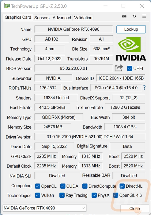
Before getting into testing I did also run GPUz to double-check that our clock speeds match up with the specifications which it did. I also have this to document the card BIOS revision as of testing as well as the driver which is the 521.90 Beta driver for before the launch.